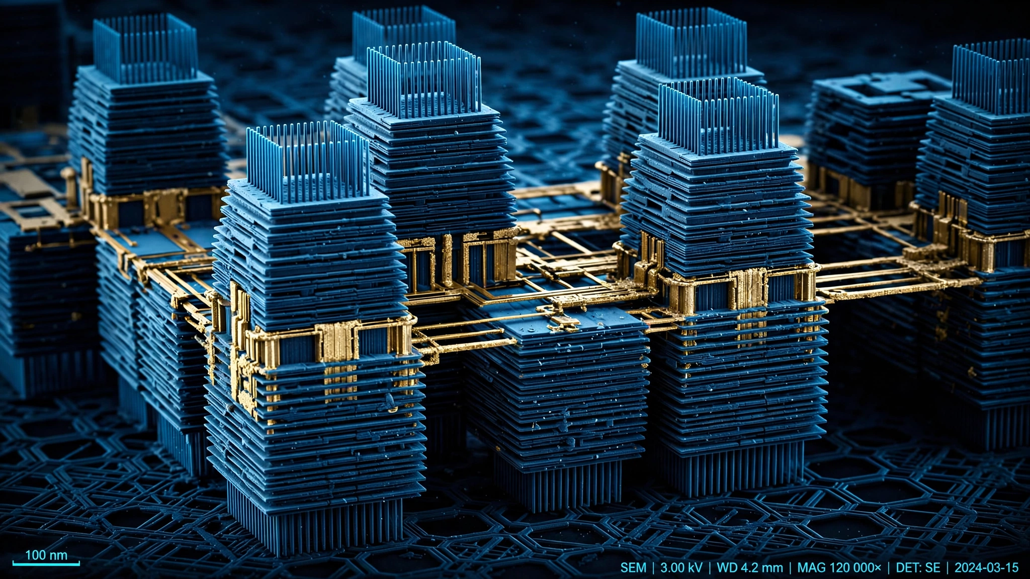
One hundred billion transistors. On a chip the size of your thumbnail. Each nanosheet is five nanometers thick, separated by nine nanometers of space, built from fifteen rows of silicon atoms. IBM announced this on June 25 at the VLSI 2026 symposium, calling it the world's first sub-1nm semiconductor technology. The node is designated 7 angstroms, or 0.7 nanometers. That is two full process generations ahead of anything any foundry on Earth has in production or has publicly committed to producing.
IBM cannot make a single one.
The $1.5 Billion Exit
In 2015, IBM did something that looked, at the time, like surrender. A company that had manufactured semiconductors for half a century transferred its chip fabrication operations to GlobalFoundries. Not sold. IBM paid GlobalFoundries $1.5 billion to take the fabs off its hands, plus an additional $600 million in cash and assets to sweeten the arrangement. East Fishkill, New York; Burlington, Vermont; the workforce; the liabilities. Gone. IBM retained only one thing: its Albany Nanotech Complex, a 300mm research fab where scientists prototype the future of transistor architecture without the burden of manufacturing chips anyone would actually buy.
The deal was messy, and it stayed messy for years: IBM sued GlobalFoundries in 2021, alleging breach of contract, GlobalFoundries countersued, and the litigation dragged on until January 2025, when both sides settled for undisclosed terms. By the time the lawyers finished, the strategic picture had clarified in a way nobody predicted at the signing. IBM Research Albany was producing breakthrough after breakthrough in transistor architecture, and every leading foundry on the planet was manufacturing variations of IBM's designs.
What Nanostack Actually Is
Current leading-edge chips use nanosheet transistors, also called gate-all-around (GAA) architecture, and Samsung shipped them first at its 3nm node in mid-2022, with TSMC following at N2 in late 2025. In both cases, the core idea came from IBM's Albany lab, which demonstrated nanosheet FETs in 2017, and every leading foundry now builds some version of IBM's design.
Nanostack goes further by abandoning the assumption that transistors must sit side by side on a flat plane. IBM stacks two layers of nanosheet transistors vertically and staggers them so the upper layer is offset from the lower. Each transistor is contacted independently: the front side carries signal connections, the backside carries power delivery, and because the two layers are fabricated separately before bonding, the top and bottom FET channels can use different materials optimized for different performance characteristics.
The key manufacturing trick is what IBM calls "ultra-thin dielectric bonding," a single bonding step that fuses the two transistor layers together with a dielectric layer thinner than the transistors themselves, which is architecturally distinct from Intel's 3D stacking discussion at its 2023 analyst day and from Huawei's "LogicFolding" concept that bonds two separate wafers after fabrication. IBM's approach is monolithic: the stacking process happens within a single wafer fabrication flow, not as a post-fabrication bonding of two finished wafers, and that distinction matters enormously for yield because every additional handling step compounds defect rates exponentially at this scale.
Performance claims are significant but carefully scoped: IBM reports up to 50% more performance or 70% greater energy efficiency compared to its own 2nm technology, and at VLSI 2026 researchers from Albany presented a 40% improvement in SRAM cell scaling confirmed by a functional CMOS inverter built using the nanostack process. A working inverter is not a working processor, but it is the fundamental logic gate that everything else is built from, the atomic unit of digital computation, and it functions. The physics works.
The Widening Transfer Gap
Here is the calculation nobody is running. IBM has been inventing transistor architectures for decades, and other companies have been manufacturing them. That handoff takes time, and the time is growing.
| IBM Innovation | Lab Demo | First Foundry Production | Transfer Time |
|---|---|---|---|
| Strained silicon (SiGe) | 2001 | AMD 90nm, 2004 | 3 years |
| High-k/metal gate | 2004 | Intel 45nm, 2007 | 3 years |
| Nanosheet/GAA FET | 2017 | Samsung 3nm, June 2022 | 5 years |
| 2nm test chip | May 2021 | Rapidus 2nm, target H2 2027 | 6.5 years* |
| Nanostack (0.7nm) | June 2026 | ??? | ??? |
*If Rapidus hits its target, which Engadget noted may be optimistic given Rapidus has never shipped a commercial chip.
The pattern is unmistakable: three years in 2004, five years in 2022, six and a half years for 2nm if Rapidus delivers on schedule. The gap is widening by roughly 1 to 1.5 years per architectural generation, and the reason is straightforward: each successive node demands more extreme manufacturing capabilities, where strained silicon required process tweaks, high-k/metal gate required entirely new materials, nanosheets required fundamentally new transistor geometries, and sub-1nm nanostack requires all of that plus 3D bonding at atomic precision, high-NA EUV lithography that only ASML can supply, and yield optimization for a manufacturing process nobody has attempted.
Extrapolating the trend: 7.5 to 8 years puts nanostack production at 2033 to 2034. IBM says five years, but IBM said its 2nm technology would be ready for production "within a few years" when it announced it in May 2021, and Rapidus, IBM's manufacturing partner, is targeting H2 2027 for 2nm, which is six and a half years, not "a few." IBM's production estimates have been consistently optimistic by 1.5 to 2 years across the last two generations.
Where This Leaves the Roadmap
TSMC plans its A14 node (1.4nm) for mass production in 2028, Samsung has pushed 1.4nm to 2029, and Intel's 14A (1.4nm) timeline remains publicly uncertain after the company deprioritized it, which means IBM's 7A sits two full nodes beyond every committed production target on Earth. Even if IBM is right about five years, the industry would not see sub-1nm chips in commercial products until 2031 at the earliest, and if the historical transfer curve holds, 2033 is the more defensible estimate.
None of this diminishes what IBM built, and the competitive landscape makes that clear: Intel discussed 3D stacking in 2023 and has not shipped it, Huawei's LogicFolding concept uses a two-wafer bonding approach that is fundamentally more complex and expensive than IBM's monolithic process, and Samsung's 3nm GAA yields were reportedly under 20% at launch. IBM has demonstrated a working nanostack CMOS inverter with validated SRAM scaling, which is further than anyone else has gone at this density.
The Strongest Case Against
The strongest argument against getting excited about IBM's nanostack is that IBM is a research lab that has permanently lost the ability to verify its own designs at manufacturing scale. When IBM had fabs, it could iterate between design and production, discovering and solving yield problems in real time. Now it publishes papers, builds prototypes in Albany, and hands the blueprints to foundries that must independently solve the hardest part of chipmaking: making billions of transistors work at once, on every wafer, thousands of times a day.
Rapidus, IBM's primary manufacturing partner for advanced nodes, is a Japanese startup founded in 2022. It has never shipped a commercial semiconductor. Its 2nm fab in Chitose, Hokkaido is under construction. Rapidus's total committed public funding stands at roughly $11.5 billion as of mid-2026, predominantly from the Japanese government. For context, TSMC spent $29.8 billion on capital expenditure in 2024 alone. Building a functional CMOS inverter in a research fab staffed by some of the world's best semiconductor physicists and then handing the process to a startup foundry that has never run a production line is a fundamentally different challenge than proving the physics works.
Samsung's experience is instructive. When it launched 3nm GAA in June 2022 using nanosheet architecture that IBM pioneered, initial yields were low enough that major customers including Qualcomm and Nvidia chose to stay with TSMC's older but higher-yielding 4nm FinFET process. Architecture is necessary but not sufficient. Manufacturing execution is what ships chips.
What This Analysis Does Not Cover
This article's transfer-time calculation relies on publicly announced dates for IBM lab demonstrations and foundry production starts. IBM's internal milestones, which often precede public announcements by 12 to 18 months, are not reflected. The trend line uses four data points across 25 years, which is enough to observe a directional pattern but not enough for high-confidence extrapolation. Cost-per-transistor data, which would strengthen or weaken the production timeline estimate, is not publicly available for any node beyond TSMC's 3nm. The SRAM scaling and CMOS inverter results reported at VLSI 2026 have not yet been independently replicated. IBM's production timeline estimate of five years may account for manufacturing variables that the historical trend does not capture, including IBM's recent acquisition of a high-NA EUV tool for Albany and its deepening relationship with Rapidus.
What You Can Do
If you work in semiconductor design, read the two VLSI papers. S. Reboh et al., "NanoStack Transistor Architecture for CMOS 7A Node and Beyond" (VLSI 2025) covers the architecture and process. Chen Zhang et al., "Area and Performance of Staggered-Channel Nanostack SRAM Bitcells" (VLSI 2026) covers the density claims. The IEEE digital library has both. These are the primary sources behind every headline, and the gap between what the papers actually demonstrate and what news coverage implies is worth understanding firsthand.
If you buy or specify chips for products shipping in the 2028 to 2032 window, plan around TSMC N2 and Intel 18A. Those are the nodes that will be in volume production. Sub-1nm is not coming to your product roadmap this decade unless you are designing for 2033 or later.
If you invest in semiconductor companies, the stock to watch is not IBM. IBM's semiconductor licensing revenue is buried inside its infrastructure segment. Companies that will capture value from nanostack are the foundries that license it, the EDA vendors (Synopsys, Cadence) that build the design tools for 3D architectures, and the equipment makers (ASML, Lam Research, Tokyo Electron, SCREEN) who build the machines that make the process physically possible. ASML is the single-supplier bottleneck for high-NA EUV. There is no second source.
The Bottom Line
IBM invented the nanosheet transistor architecture that every leading foundry now manufactures. It invented strained silicon before that, and high-k metal gates before that. Now it has demonstrated the first sub-1nm chip technology, two full nodes ahead of the production frontier. It did all of this from a research lab in Albany, New York, with no manufacturing capability of its own, after paying $1.5 billion to exit the business of actually making chips. IBM's transfer time from lab to foundry production line has grown from three years in 2004 to a projected seven or eight years for nanostack. That widening gap is not IBM's failure. It is a measure of how hard chipmaking has become, how much more extreme each generation of manufacturing needs to be, and how few organizations on Earth can do it at all. IBM builds the future of computing. It just takes everyone else the better part of a decade to catch up.