The $2 Billion Invisible Defect Tax Hiding Inside Every AI Chip
NVIDIA spends roughly $1,000 per B200 GPU on yield failures that no one can diagnose without destroying the chip. A Munich startup using nitrogen-vacancy centers in synthetic diamond just secured €76 million in EU backing to map current flow through sealed 3D packages, and the value of that visibility starts at $127 million for every percentage point of yield recovered across the advanced packaging industry.
One thousand dollars. That is the yield-loss cost baked into every single NVIDIA B200 GPU that rolls off the production line, according to Epoch AI's bill-of-materials breakdown of the chip's $6,400 total production cost. Sixteen percent of that manufacturing cost goes straight into the garbage. Defective dies, broken microbumps, misaligned through-silicon vias buried inside sealed 3D packages cannot be found, diagnosed, or repaired with any tool in commercial production today.
That number landed differently on June 23, when the European Commission approved €76 million in German state aid for QuantumDiamonds GmbH, a TU Munich spinoff building the first production-scale quantum diamond microscopy systems for semiconductor inspection. Buried in the Commission's evaluation was a phrase that should make every KLA shareholder sit up: QuantumDiamonds "has the potential to create the next ASML." Coming from the same institution that governs the European Chips Act's €43 billion allocation, that is not a throwaway line.
Where the Money Disappears
Advanced packaging has quietly become the most expensive step in making an AI chip. Not designing the logic. Not fabricating the silicon. Assembling the stack. Five lines from the B200's bill of materials tell the story:
| Component | Cost | Share of BOM |
|---|---|---|
| HBM memory | $2,900 | 45% |
| Advanced packaging | $1,100 | 17% |
| Yield loss | $1,000 | 16% |
| Logic die (GPU silicon) | $900 | 14% |
| Other | $500 | 8% |
| Total | $6,400 | 100% |
Packaging plus yield loss together account for 33 percent of the chip's production cost. Those two categories are deeply entangled in ways that make solving one dependent on solving the other. Nobody has solved either. When TSMC's CoWoS process stacks HBM memory dies on top of a GPU logic die with hybrid bonding at 9-micrometer pitch, the first-pass yield for that assembly runs between 78 and 85 percent, according to Mordor Intelligence's 2025 production data. Conventional semiconductor fabs, fabricating monolithic dies on flat wafers inspected at every layer by tools with decades of refinement behind them, routinely achieve yields above 95 percent. That gap is enormous, and it persists because every inspection tool available in production today was designed for flat, unsealed wafers, not for multi-die stacks sealed inside packages where the failures hide.
"Non-destructive fault isolation in advanced packaging is an incredibly difficult challenge," Dr. David Su, former director of TSMC's failure analysis team and now a QuantumDiamonds advisor, told SemiEngineering. Every option currently available is bleak, and the reasons are fundamental rather than engineering obstacles waiting to be optimized away. Lock-in thermography detects hotspots but cannot resolve individual current paths, X-ray computed tomography sees physical structures but is entirely blind to electrical behavior, and neither technology can tell you whether current is actually flowing through the connections that hold a $6,400 chip together. Scanning electron microscopy requires cracking the package open, which is roughly equivalent to performing an autopsy to diagnose a living patient: you get your answer, but you have destroyed the thing you wanted to save.
Calculating the Defect Tax
Nobody had published the aggregate dollar cost of this inspection gap for a single chipmaker. So here it is.
NVIDIA shipped approximately 2 million B200 graphics processing units in 2025, an estimate grounded in FourWeekMBA's analysis of NVIDIA's data center revenue and average selling prices, making it the single largest consumer of advanced packaging capacity on Earth. At $1,000 of yield loss per unit, that represents roughly $2 billion per year in manufacturing waste for one company building one product. AMD's MI300X and forthcoming MI400 series, Google's TPU v6, and Amazon's Trainium 2 all use comparable advanced packaging processes with similar yield profiles. Add it up across the industry. Five billion dollars a year, gone.
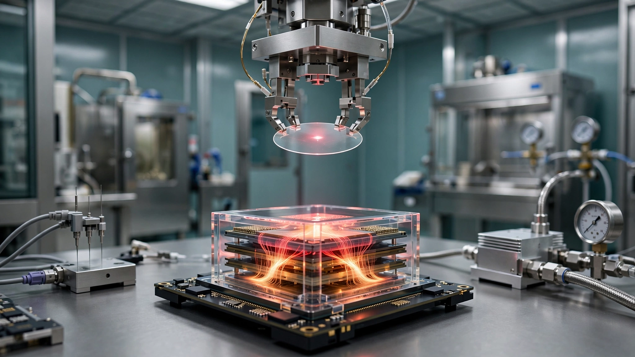
Now layer QuantumDiamonds' capability on top of that number. Here is how it works. Quantum diamond microscopy uses nitrogen-vacancy centers in synthetic diamond, atomic-scale defects where a nitrogen atom and an adjacent vacancy in the crystal lattice form a quantum sensor that fluoresces in response to magnetic fields. Current flowing through a microbump or TSV generates a magnetic field that NV centers detect with a sensitivity no other sensor technology can match at room temperature and atmospheric pressure. What emerges is a spatial map of every active current path in the package at micrometer resolution, through the sealed lid, within seconds, without decapping, without destruction, and without any of the guesswork that defines current failure analysis workflows.
If that capability reduces yield loss by just 5 percent, the savings per chip are $50. Across NVIDIA's 2 million annual B200 units: $100 million per year from a single product line. Extend the calculation to all four major AI chip manufacturers using advanced packaging and the addressable savings land between $300 million and $500 million annually.
Scale the lens wider. Scale the calculation across the full market and the numbers compound fast: advanced 2.5D and 3D packaging reached $12.73 billion in 2026, projected to hit $24.18 billion by 2031 at 13.69 percent CAGR. Every single percentage point of yield improvement across that market, moving from 84 to 85 percent or from 87 to 88 percent, recovers $127 million in product value that currently leaves the factory floor as waste. Moving from 85 percent yield to 88 percent recovers $380 million per year at current volumes, and volumes are doubling within five years.
Why "Next ASML" Is a Structural Comparison, Not Hype
ASML spent two decades as a small Dutch lithography company building tools that nobody else wanted to commercialize. Today it commands a $350 billion market cap and holds a monopoly so complete that every leading-edge chip fabricated on Earth, from the processors inside iPhones to the accelerators training frontier AI models, passes through an ASML tool at least once during manufacturing. KLA followed a parallel trajectory in inspection and metrology, reaching $349 billion in market capitalization on $12.2 billion in trailing revenue by owning the chokepoint of defect detection: if you need to find flaws in your silicon during manufacturing, you buy KLA's tools or you buy nothing.
KLA's advanced packaging process control revenue reached roughly $635 million in 2025 and is projected to exceed $1 billion in 2026, a 57 percent year-over-year surge that reveals how desperately fabs need better visibility inside stacked packages. But even KLA cannot do what QDM does. Not yet. KLA inspects surfaces, layers, physical geometry, and it does so brilliantly, but it cannot map live current flow through a sealed package without destroying the very thing the customer paid $6,400 to build.
QuantumDiamonds fills a capability gap that no existing tool at any price addresses, a fact underscored by nine of the ten largest chip manufacturers completing proof-of-concept evaluations with the company despite its pre-revenue status. Systems are deployed at Eurofins EAG Labs in Sunnyvale and iST in Hsinchu, Taiwan, two of the industry's most respected independent failure analysis houses. That €76 million in state aid anchors a €152 million total investment plan to build the company's first production-scale facility in Munich, a city already home to the Technical University of Munich physics department where the underlying NV-center research originated and where the local talent pipeline for quantum engineering runs deep.
That parallel is structural, not aspirational, and it rests on a specific characteristic shared by both technologies. EUV lithography succeeded because it was the only path forward for shrinking transistors below 7 nanometers, and every alternative hit fundamental physical limits that no amount of engineering could circumvent. QDM may occupy the same position for 3D package inspection: the only non-destructive technology that maps electrical behavior, not just physical geometry, inside sealed multi-die stacks. Whether that monopoly potential survives first contact with KLA's acquisition department, which has spent three decades buying exactly this kind of promising inspection startup and folding it into the platform before it can build independent traction, is the question that determines whether QuantumDiamonds becomes a company or a product feature.
Chiplets Make It Worse
Monolithic dies are giving way to chiplet architectures. Every additional die in the stack multiplies the inspection challenge exponentially, which matters because CoWoS capacity runs at over 90 percent utilization consumed almost entirely by four companies, NVIDIA, Google, AMD, and Amazon, and every one of them is demanding more dies per package, not fewer. As those customers demand larger interposer sizes and higher die counts, the number of microbumps, TSVs, and hybrid bonds per package is climbing from tens of thousands to hundreds of thousands, and each connection is a potential failure point invisible to every tool except QDM.
"Substantial die-to-die process variation in chiplet packaging reduces the reliability of conventional golden-die and die-to-die inspection," Woo Young Han of Onto Innovation observed in SemiEngineering's chiplet inspection analysis. IEEE 1838 reserves up to 8 percent of through-silicon vias for probing access, yet even that allocation falls short of 95 percent defect coverage, which is roughly equivalent to probing 8 percent of a building's wiring and expecting to find the short circuit that eventually burns it down.
Limitations
QuantumDiamonds is pre-revenue and has not disclosed production system pricing. A 5 percent yield-improvement figure used in the defect tax calculation is a projection based on the nature of the tool gap QDM addresses, not a measured outcome from any manufacturing deployment. No proof-of-concept evaluation with a major chipmaker has produced publicly available yield-improvement data, so the economic case rests on the logical chain from "invisible defects cause yield loss" to "making them visible reduces yield loss" without empirical confirmation of the magnitude. NVIDIA's per-unit yield cost of $1,000 derives from third-party BOM analysis by Epoch AI and FourWeekMBA, not from NVIDIA's own disclosures; actual internal yield accounting is proprietary and may differ materially. NV-center quantum sensing is established physics, but manufacturing-floor deployment at the throughput and reliability required for inline production inspection remains undemonstrated at scale. Matching private investment behind the €76 million in state aid carries terms and conditions that have not been disclosed publicly.
Strongest Case Against
KLA is not asleep. Record quarterly revenue of $3.42 billion in Q3 FY2026 and is actively developing AI-driven defect classification, advanced infrared inspection, and X-ray tomography engineered specifically for 3D packaging. KLA has spent decades embedding its tools and software ecosystem in every major production line on Earth, creating switching costs measured in years and hundreds of millions of dollars. When a genuinely useful new inspection modality emerges, the historical pattern is acquisition and integration: KLA buys the technology, ships it as a module of an existing platform, and leverages its installed base to achieve adoption faster than any startup could on its own. QuantumDiamonds' €152 million total investment plan is a rounding error against KLA's $12.2 billion annual revenue. ASML succeeded because EUV was the only possible path forward for transistor scaling, full stop. QDM is one of several approaches to packaging inspection, and KLA is pursuing most of the others simultaneously with vastly more resources and infinitely deeper customer relationships. Whether the quantum diamond gap is wide enough to sustain an independent company, rather than becoming a $500 million acquisition that KLA absorbs and ships as a feature, is the question that €76 million in state aid does not answer.
What You Can Do
If you manage a semiconductor fab or outsourced assembly and test facility running advanced packaging, request a QuantumDiamonds proof-of-concept evaluation now, during the phase when the company is still proving its technology broadly and evaluations carry favorable terms. Nine of the ten largest chipmakers have already completed theirs. Compare QDM's current-mapping output directly against your existing failure analysis workflow on a batch of packages with known defect modes, and measure whether the tool catches failures your current inspection stack misses. If it does, the yield-improvement percentage you observe becomes the most valuable number in your procurement decision, because it converts directly to dollars saved per unit shipped.
If you invest in semiconductor equipment, watch KLA's next two earnings calls for any language about quantum sensing, non-destructive current mapping, or NV-center technology. Silence from KLA on this topic is itself a signal worth trading on. If KLA starts discussing it, they are building or buying, and the acquisition premium for QuantumDiamonds starts climbing. If they do not mention it, the gap may be wider than the incumbents are willing to acknowledge publicly, and QuantumDiamonds' next funding round becomes significantly more interesting. Track whether any of the nine chipmaker PoCs convert to production purchase orders, because that transition is the proof point that separates laboratory demonstration from manufacturing necessity.
If you design chiplet-based products, factor inspection access into your package architecture at the design stage. Creating power domains that can be individually driven for QDM imaging, standardizing test-current injection points, and ensuring thermal paths do not obstruct diamond sensor placement costs almost nothing during design but determines whether a finished package is inspectable or remains a sealed black box that fails silently and expensively.
The Bottom Line
For a decade, the semiconductor industry perfected the art of stacking silicon dies into skyscrapers, connecting them with forests of microscopic vertical wires, and sealing the results inside packages that no existing tool can see into without breaking open. Building the skyscrapers worked. Inspecting them did not. That failure has a price tag. NVIDIA alone pays $2 billion a year in chips that fail for reasons nobody can diagnose, and industry-wide, that toll exceeds $5 billion and will grow as advanced packaging volumes double by 2031. A synthetic diamond the size of a fingernail, engineered with atomic-scale defects that glow red when current flows nearby, can look inside those sealed stacks and map what is happening without cracking a single seal. Whether QuantumDiamonds becomes the next ASML or the next acquisition target, the capability it represents will become as mandatory for packaging as lithography is for transistors. This tax has an expiration date. Who collects the refund is the only question left.